
The "Blameless" Amplifier is a high-performance audio power amplifier design developed by British engineer Doug Self. The design was first conceived around 1997 as part of Self's work on reducing distortion and improving the linearity of solid-state audio amplifiers. It became particularly well known through his book Audio Power Amplifier Design and subsequent refinements of the circuit.
The name "Blameless" comes from Self's approach to amplifier design and distortion analysis. Rather than blaming a single component or stage for the amplifier’s distortion, the design aims to ensure that no individual stage is operating in a way that unnecessarily contributes significant distortion. Each stage is carefully designed and biased so that the overall amplifier achieves very low distortion through the combined performance of all its stages.
The Blameless Amplifier is therefore less a single fixed circuit than a design philosophy and topology. It incorporates techniques such as a highly linear voltage amplification stage, carefully controlled biasing, emitter degeneration, local feedback and a well-designed output stage. The result is an amplifier that can achieve extremely low levels of distortion while remaining relatively straightforward to build and understand.
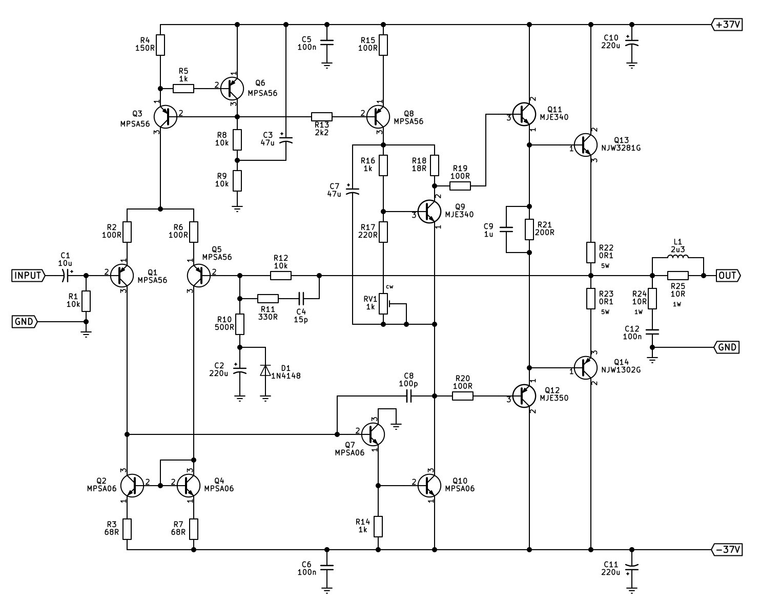
Circuit Description
The input signal is applied to Q1, while Q5 receives the global negative-feedback signal from the output. Q1 and Q5 therefore form the long-tail differential pair (LTP). Q3 provides the approximately 4.3 mA tail current, with Q6 and C3 forming the bootstrapped voltage reference that keeps the current source relatively insensitive to supply-voltage variations. That 4.3mA is actually rather high for this stage; reducing the LTP current to around 1mA is generally preferable because it reduces input-stage distortion and noise contributions without sacrificing useful performance.
Q2 and Q4 form the current mirror for the LTP. The mirror converts the differential current from the two transistors into a single-ended signal, providing a higher effective load and increasing the gain of the input stage.
The signal then drives Q7 and Q10, which form the beta-enhanced voltage amplification stage (VAS). The beta enhancement substantially improves the linearity of the VAS by providing local feedback around the voltage-amplifying transistor. Q8 supplies the VAS with a relatively constant current of about 6mA. This stage provides most of the amplifier's open-loop voltage gain.
Q9 is the VBE multiplier, or bias spreader. Its job is to establish and control the voltage between the driver transistor bases, thereby setting the quiescent current of the Class-AB output stage. It should be in good thermal contact with one of the drivers (either Q11 or Q12) so that the bias tracks temperature. Doug actually bolted it directly to the face of one of the drivers in his final PCB version.
Q11 and Q12 are the driver transistors, which provide the current gain necessary to drive the output devices. Q13 and Q14 form the complementary emitter-follower output stage. The output transistors provide the required load current while having relatively little voltage gain themselves. The 0.1 ohm emitter-degeneration resistors help equalise current sharing and improve the linearity and thermal behaviour of the output stage.
D1 is not there as part of the normal signal amplification. Its primary purpose is to protect C2, the 220u electrolytic capacitor, from being subjected to reverse voltage.
During an abnormal condition (particularly when the amplifier is driven hard into clipping or suffers a fault), the voltage at the base of Q5 can swing negative. Without D1, C2 could then be reverse-biased. Electrolytic capacitors don't like this, and significant reverse voltage can damage them.
D1 therefore acts as a clamp. When the base of Q5 attempts to go more than roughly 0.6–0.7 V negative relative to ground, D1 conducts and prevents the voltage from going much further negative.
And this is where D1 can be considered a bad idea, at least from a purist Blameless-design perspective.
A diode is a highly non-linear device. The moment Q5's base reaches the diode's conduction threshold, D1 suddenly changes from essentially an open circuit into a conducting device. Consequently, instead of allowing the LTP/VAS to behave in a predictable, linear fashion during overload, D1 introduces a hard non-linear clamp into the signal path.
Under normal operation it does essentially nothing, so it has virtually no effect on the normal THD performance. But during large-signal excursions it can conduct heavily, injecting current into a sensitive part of the amplifier. When the signal subsequently comes back inside the clamp region, the diode has to turn off again, and the stored charge and recovery behaviour can contribute to overload recovery distortion.
So D1 represents a classic engineering compromise: it protects C2 during a fault or severe overload, but introduces a non-linear element into a very sensitive part of the amplifier whenever it conducts. If C2 is adequately protected by other means, or if a suitable non-polarised capacitor is used, the diode can be unnecessary. Self was particularly interested in avoiding these apparently small non-linearities because the whole point of the Blameless methodology is to eliminate such avoidable error mechanisms.
R12 is the main global feedback resistor, connecting the amplifier output back to the inverting input (Q5). This establishes the DC and low-frequency feedback path.
R11 and C4 are connected in parallel with R12, but with C4 in series with R11. At low frequencies C4 is effectively an open circuit, so R12 dominates and the normal feedback network determines the amplifier's closed-loop gain.
As frequency increases, the impedance of C4 falls. R11 and C4 therefore progressively provide an additional, much lower impedance feedback path around R12. In other words, negative-feedback is increased at high frequencies, causing the closed-loop gain to roll off.
R11 is important because it prevents C4 from becoming a virtually direct AC short between the output and the differential-pair input. It limits the high-frequency feedback current and, together with C4, establishes a controlled frequency response rather than simply dumping a capacitor across R12.
This network is therefore part of the amplifier's high-frequency compensation and stability strategy. It deliberately shapes the feedback loop so that the amplifier has reduced gain at very high frequencies, helping prevent unwanted phase-shift-related instability and parasitic oscillation.
So, in very simplified terms:
R12 sets the main feedback ratio, while R11/C4 progressively increases the feedback at high frequency and rolls off the closed-loop gain.
That little R11/C4 network is a good example of the Blameless philosophy; rather than simply accepting whatever high-frequency behaviour the transistor stages happen to produce, the feedback network is deliberately shaped to keep the complete amplifier well behaved.
Doug's “load-invariant” (Blameless) amplifier
Aptly named "load-invariant" amplifier because of its performance - such as its frequency response, voltage output, or low distortion level - remains constant (invariant) regardless of changes in the electrical impedance (the "load" or speaker) connected to its output.
Please note that I have only simulated the figure 1 schematic (as printed in his book) and have not physically built or tested either version.
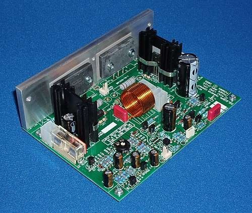
Considering the PCB is nearly $60 AU for one, I have no real intention of purchasing or building one of these; nor reverse-engineering it to see if matches the below schematic exactly.
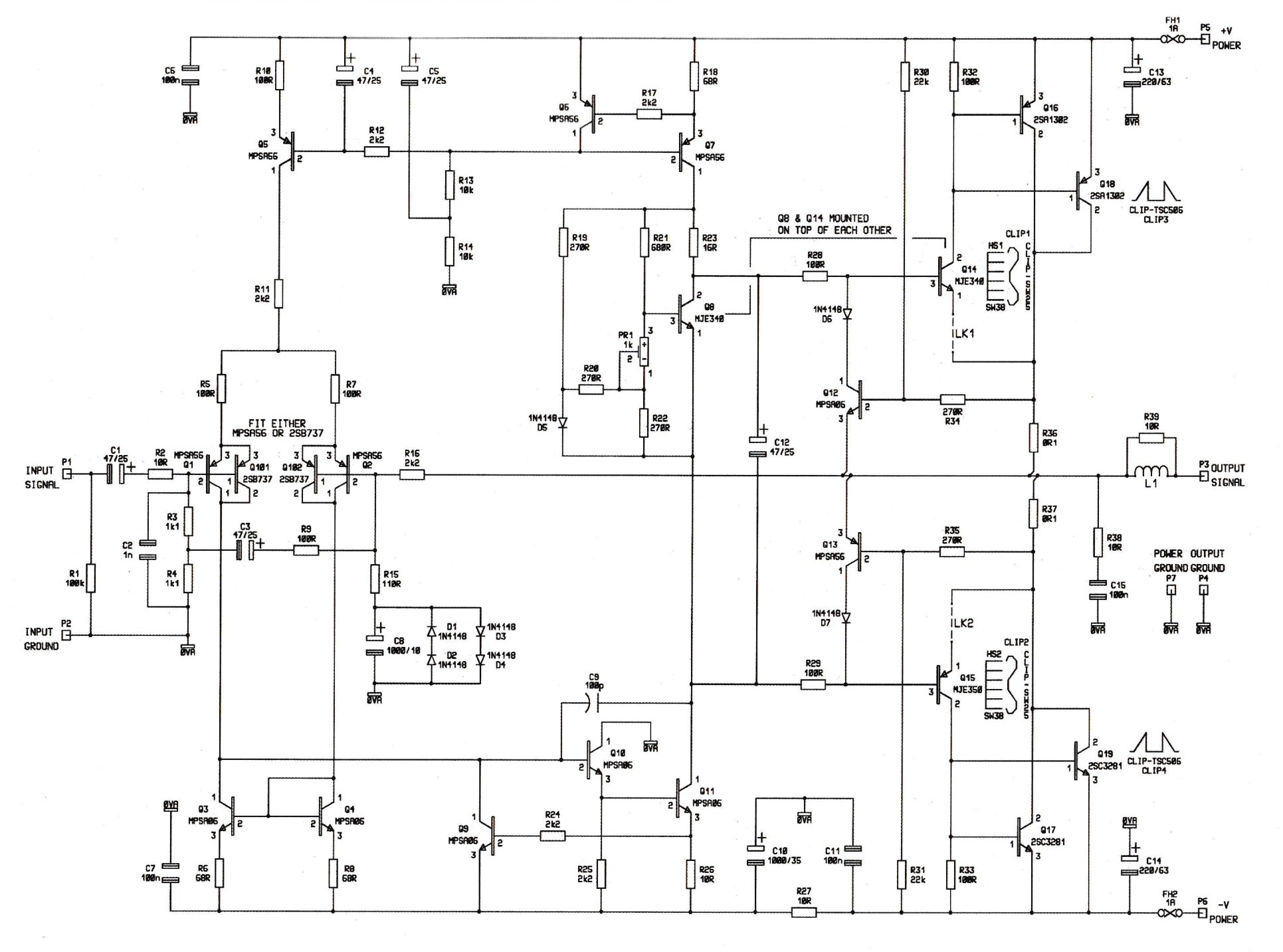
There are a few differences in this schematic to the one in figure 1. For one, the output stage is a complimentary-feedback pair (CFP) compared to emitter-follower (EF). The other difference is the input stage; a "doubled-up" long-tailed pair. Where two transistors on either side of the differential are wired in parallel. The main purpose of doing this is to lower the amplifier's overall internal noise (often referred to as Johnson or thermal noise).
It also lowers the equivalent base resistance of the single transistor. A major source of noise in bipolar junction transistors (BJTs) is the internal base spreading resistance. When you wire transistors in parallel, their internal base resistances are placed in parallel. Paralleling two transistors halves the total equivalent base resistance, which directly dictates a quieter input stage.
Another interesting point is the sheer size of the inductor coil. 1 inch diameter (approx. 26mm). 1 inch! It's made up of 10 turns of 18 AWG (approx. 1.24mm diameter) enameled-copper wire with an overall diameter of 1 inch. This, according to an inductance calculator, puts its inductance at around 2.3µH. This may "seem" a little on the large size, inductance-wise; but I have seen some amplifiers with output inductors of up to 10µH. Thanks goes to a mate for providing a better scanned copy of the original magazine schematic.
For those interested in purchasing the PCB, you can find it at The Signal Transfer Company's website, among other things as well.
Specifications of the current Blameless amplifier
Power output: from 25W to 100W into 8 Ohms, depending on supply voltage. Assumes adequate heatsink.
Power supply: +/-24V to +/-45V
Distortion: <0.0006% at 1kHz, 25W/8R. <0.003% at 10kHz, 25W/8R.
Noise out: <-95 dBu (22-22kHz bandwidth, RMS, source resistance 50 ohm)
Gain: 23 times (+27.2 dB)
Frequency response: +/-0.1 dB, 10Hz - 20kHz
Input impedance: 2.2k without bootstrapping, 10k with bootstrapping option
Conclusion
The Blameless amplifier demonstrates that achieving extremely low distortion does not require exotic circuitry, but rather careful attention to every stage of the amplifier. By making each stage inherently linear, controlling bias currents, using local feedback where appropriate, and ensuring that no individual device is unnecessarily contributing distortion, the overall amplifier can achieve excellent performance while remaining relatively simple and practical (albeit the 1997 schematic seems a little convoluted; especially the input stage).
The name "Blameless" is therefore particularly appropriate: instead of having one stage to blame for the amplifier's shortcomings, the design philosophy is to make every stage behave itself.