
I stumbled upon this circuit while randomly searching for using the 555 timer IC as a crude amplifier, which has been done before. This was a concept circuit published on ElectroBob as a 555 Class-D amplifier. Whereas the amplifier part barely works, and draws a substantial idle current (~600mA at 12V); I found the "home-made 555" circuit interesting.
Firstly, as a refresher, I've shown the standard DIP-8 NE555 timer block-diagram below from Texas Instruments.
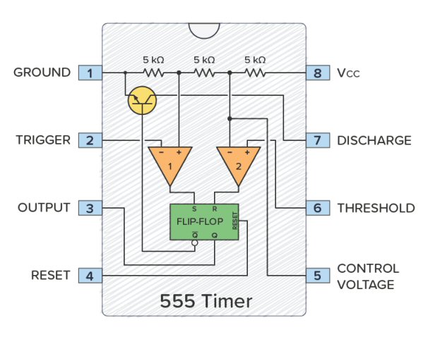
Knowing the internal workings of the 555, and also forgetting the misconception that it was named after the three 5k resistors in the voltage divider (they were actually chosen at random); we'll now look at Bogdan's high-current 555 implementation.
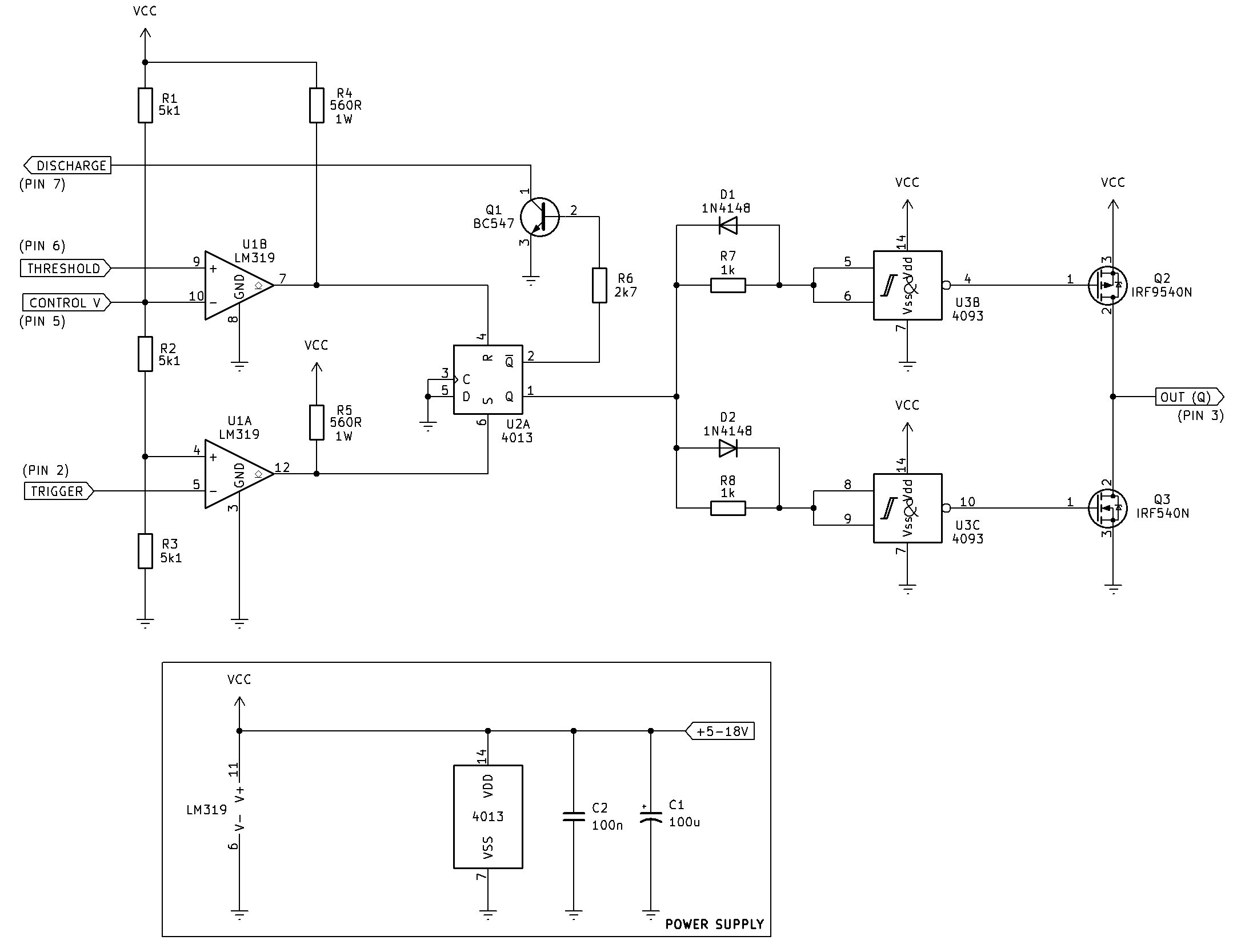
Using the original circuit as published, it doesn't work as it fails to oscillate. It turns out the schematic was drawn wrong around the 4013 flip-flop, where the NOT Q (Q with a line above it, meaning its logic output is inverted - and will be continued to be referred to as "NOT Q" for the rest of this article) was connected to the MOSFET gate-drive circuit (U3), instead of the discharge transistor (Q1). What this meant was, on "start-up", Q1 was conducting forcing a discharge output - therefore it could never charge an external capacitor if configured in astable mode; resulting in it never being able to oscillate in the first place.
A supply voltage of 18V DC is the absolute maximum and should not be exceeded as that's the maximum supply voltage of the 4093 IC. Incidentally, the maximum voltages for the LM319 and 4013 are 36V and 20V respectively. On the low-end of the spectrum, the voltage should not be lower than 5V DC as this is the minimum operating voltage of the the LM319.
Circuit Description
The timing and threshold section is based around the two sections of the LM319. R1, R2 and R3 form a resistor network that establishes the reference voltages for the two comparators. The arrangement is analogous to the two-thirds-VCC and one-third-VCC reference levels found in a conventional 555, although here the actual thresholds are determined by the resistor network and the applied control voltage at pin 5. The upper comparator, U1B, monitors the THRESHOLD input at pin 6, while the lower comparator, U1A, monitors the TRIGGER input at pin 2.
U1A is responsible for setting the flip-flop. Its non-inverting input is connected to the internal reference while its inverting input receives the trigger signal. When the trigger voltage falls below the lower threshold, the comparator changes state and sets the 4013 flip-flop. This causes the Q output at pin 1 of U2A to change state. In this respect, U1A performs essentially the same function as the trigger comparator inside a conventional 555.
U1B performs the threshold function. Its non-inverting input receives the threshold voltage while its inverting input is connected to the control-voltage reference. When the threshold voltage rises above the upper reference level, U1B changes state. Its output drives Q1 through R6. Q1 then pulls the reset input of the 4013 low, resetting the flip-flop. The result is the familiar 555 behaviour: a sufficiently low trigger voltage sets the output, while a sufficiently high threshold voltage resets it.
The 4013 therefore acts as the memory element in the circuit. The comparators themselves only respond to instantaneous input voltages, whereas the flip-flop remembers which state the circuit should remain in between trigger and threshold events. This is an important feature of the 555 architecture. Once the trigger comparator sets the flip-flop, the output remains in that state until the threshold comparator resets it.
Q1 is a BC547 with its emitter connected to ground and its collector connected directly to the DISCHARGE (pin 7) connection. Its base is driven from the complementary output of the 4013 flip-flop through R6.
The purpose of Q1 is to provide a controlled path to ground for whatever is connected to the discharge pin. In a conventional 555, pin 7 is connected to an internal transistor that turns on when the flip-flop is reset. This circuit recreates that function externally using Q1.
When the 4013 is in its SET state, its Q output at pin 1 is high and its complementary NOT Q output at pin 2 is low. Consequently, Q1 is switched off. Pin 7 is therefore effectively open-circuit, allowing the external timing capacitor or other timing network connected to the discharge terminal to charge through its associated resistor.
When the 4013 is RESET, Q goes low and NOT Q goes high. Current flows through R6 into the base of Q1, turning it on. Q1 then pulls the DISCHARGE pin 7 almost directly to ground. Any timing capacitor connected to pin 7 can therefore discharge rapidly.
So Q1 does not reset the 4013. Rather, the threshold comparator causes the 4013 to reset, and the 4013 in turn switches Q1 on to perform the discharge function.
The Q output of the 4013 then feeds the two sections of the 4093 through R7 and R8. U3B and U3C are being used as high-speed Schmitt-trigger buffers, with their inputs tied together. Their purpose is not to provide the substantial output current themselves, but to provide clean, well-defined logic transitions and sufficient gate-drive capability for the power MOSFETs.
R7 and R8, together with D1 and D2, control the charging and discharging paths of the MOSFET gates. The resistors limit peak gate current and help prevent excessive switching transients, while the diodes provide a lower-resistance path in the opposite direction. Consequently, the turn-on and turn-off behaviour of the MOSFETs can be made different, which can be useful for controlling switching speed and reducing unwanted overlap or excessive switching noise. This is important as without the behaviour of the two NAND gates, both MOSFETs could be turned on at the same time resulting in shorting the supply rails.
The final output stage consists of Q2, an IRF9540N P-channel MOSFET, and Q3, an IRF540N N-channel MOSFET. They are connected as a complementary push-pull output stage. When the 4013 output changes to the state that commands U3B to turn on, Q2 conducts and pulls the output toward VCC. When the opposite state is commanded, U3C drives Q3 on and pulls the output toward ground. The result is a very low-impedance output capable of supplying considerably more current than the output of a conventional 555.
There is an important distinction here compared with a conventional 555, however. This circuit does not simply reproduce the 555's bipolar transistor output stage. The 4093 gates act as dedicated MOSFET gate drivers, while Q2 and Q3 supply the actual load current. The output can therefore handle substantially larger currents, subject of course to the MOSFET ratings, heatsinking and the power supply.
Note that pin 4, the "RESET" pin is not implemented. In practice, pin 4 is usually tied "high" (to Vcc) to "enable" the IC to oscillate. There's only a few circuits that implement the reset pin to specifically control the IC's operation.
The power supply section at the bottom may seem confusing (this is just how KiCad 9 represents the particular ICs), but it just shows the LM319 and the 4013 power supply pins connected to Vcc and ground for completeness. C2, the 100n capacitor, provides high-frequency decoupling close to the LM319 and 4013, while C1, the 100u capacitor, provides bulk energy storage and helps prevent supply voltage disturbances when the MOSFETs switch large currents.
Idle current is around 60mA with every "pin" open. The reason for this is the two pull-up resistors (R4 & R5) on the outputs of the two comparators of U1. The datasheet shows a 500 ohm resistor there.
Testing
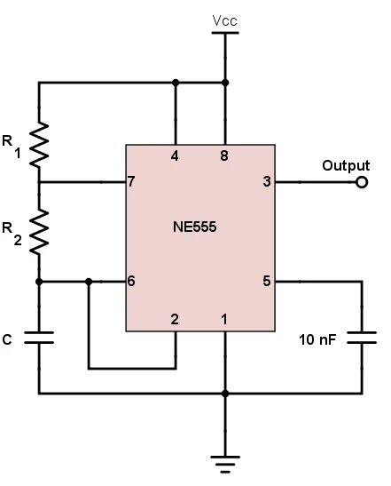
Figure 3 shows the standard astable configuration taken from the datasheet of the 555. I chose for my testing scenario 22k for R1, 47k for R2 (was just a couple of random resistors sitting on the desk!) and "C" is varied. The output is left unloaded and the current of the power supply was limited to 200mA at 12V DC.
I started with 10u for "C" which gives a rough frequency of 1.2Hz.
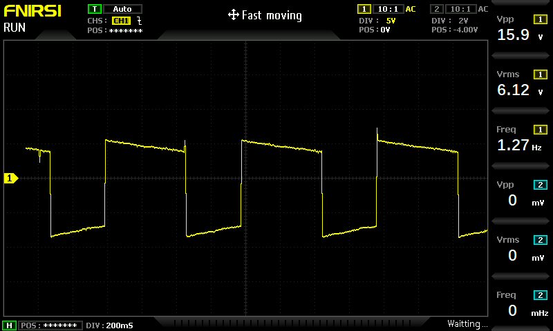
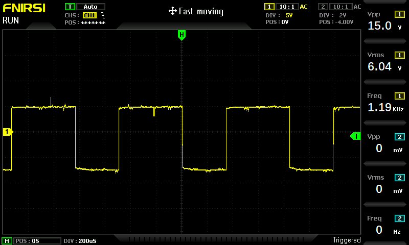
Next, I changed "C" to 10n giving a frequency of roughly 1kHz
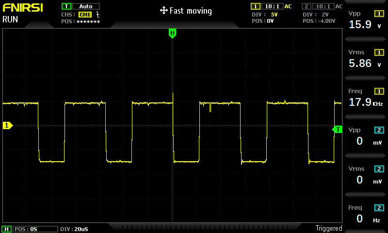
"C" was again changed to 680p which gives a rough frequency of 18kHz
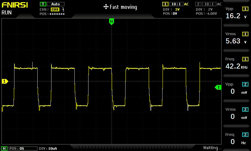
Finally "C" was changed to 220p and yields a frequency of 42kHz
Conclusion
What is the point to this? None, really. But it does show how the fundamental circuitry inside the humble 555 timer IC works - plus, it's a fun experiment. Why the high currents with the output unloaded, though? The answer is simple, the extra ~136 mA at 42 kHz is predominantly the price of repeatedly switching the large IRF540N/IRF9540N pair with relatively weak 4093 gate drive. The fact that we're seeing nearly 200mA with no external load strongly points toward switching/shoot-through losses. Which means this is a combination of MOSFET gate-charge current, 4093 output-stage current and, most importantly, shoot-through current in Q2/Q3 during their finite switching transitions.
Whereas this circuit is interesting, it's not really practical. A standard 555 timer with a "boost" transistor (like a low-side switch) on the output is a better approach to providing high-current to a load.