
This is a bipolar (symmetrical supply) voltage-feedback audio power amplifier employing a long-tail pair input stage, a voltage amplification stage (VAS), and a quasi-complementary emitter-follower output stage. Although complementary power transistors were available when this topology became popular, high-performance PNP power transistors often exhibited poorer gain and frequency response than their NPN counterparts. The quasi-complementary output stage overcame this limitation by using identical NPN output transistors while employing additional circuitry to make the negative half of the amplifier closely emulate the behaviour of a true complementary emitter-follower stage.
With the current circuit values and a supply voltage of +/-30V, this amplifier will happily produces 40W of clean output power into an 8 ohm load with a reasonable total harmonic distortion.
Specifications (tested performance of prototype at +/-30V DC):
Output power: 42.7W into 8 ohms; 68W into 4 ohms
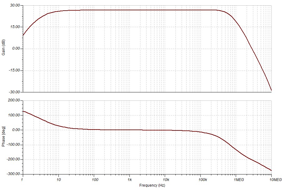
Frequency response: 15Hz - 25kHz
Input sensitivity: 1.43V RMS (full output into 8 ohms)
Total harmonic distortion (THD): <0.08% (full power into 8 ohms)
DC offset (with unmatched input transistors): ~-12mV
Stability: Unconditional
Circuit Description
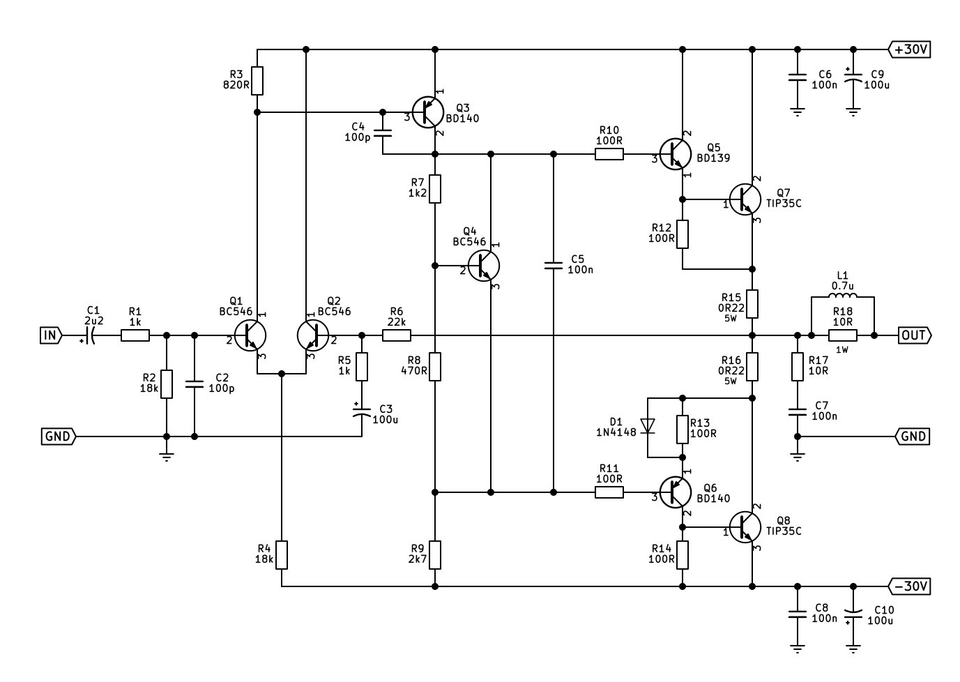
The input signal enters through coupling capacitor C1, which blocks any DC component from the source while allowing the AC audio signal to pass into the amplifier. Resistor R1 limits the input current into the base of Q1, while R2 provides the input bias path to ground. Capacitor C2 forms a low-pass RF filter with R1 and R2, preventing radio-frequency interference from entering the amplifier. Resistor R6 provides global negative feedback from the output to the base of Q2, making Q1 and Q2 operate as a differential amplifier or long-tail pair.
Q1 and Q2 form the amplifier's input stage. Q1 receives the incoming audio signal, while Q2 monitors the output voltage through the feedback network. The emitters of both transistors are tied together and fed by resistor R4 to the negative supply, establishing a tail current of approximately 1.6mA that biases the differential pair. Any difference between the voltage at the input transistor and the feedback transistor is converted into a current difference between their collectors. This is the first stage of voltage amplification and is responsible for the amplifier's excellent linearity because the feedback continually forces both transistor bases to remain at nearly the same voltage.
The collector of Q1 drives the base of Q3, which is a BD140 PNP transistor configured as the voltage amplification stage. The VAS is responsible for producing nearly all of the amplifier's voltage gain. Because only a relatively small collector current flows through Q3 (approximately 10.7mA) while it develops a large voltage swing, it can generate the tens of volts required to drive the output stage from only a few millivolts of the differential input signal.
Capacitor C4 provides miller compensation to limit the bandwidth of the amplifier in order to maintain stability. Without C4 the amplifier would have excessive high frequency gain resulting in a poor phase margin, and would almost certainly oscillate.
Q4 functions as the VBE multiplier, sometimes referred to as the bias spreader. Resistors R7, R8 and R9 sets the operating current of the VAS and in turn the output stage. This voltage compensates for the base-emitter junctions in the driver and output stages, ensuring that Q7 and Q8 conduct a small standing current when no signal is present. Correct bias adjustment minimises crossover distortion while preventing excessive idle current that could lead to overheating.
The output stage begins with driver transistors Q5 and Q6. Q5 is an NPN BD139 that drives the upper output transistor Q7, while Q6 is a PNP BD140 that controls the lower output transistor Q8. Base-stopper resistors R10 and R11 reduce the possibility of parasitic oscillation, while resistors R12, R13 and R14 assist with bias stability and base current control.
The final output devices are Q7 and Q8, both TIP35C NPN power transistors. This immediately identifies the amplifier as having a quasi-complementary output stage because both power devices are NPN transistors. Q7 operates as a conventional emitter follower on the positive half-cycle. During positive output excursions, Q5 supplies base current into Q7, causing its emitter to follow the drive voltage and source current into the loudspeaker.
The negative half-cycle operates quite differently. Since Q8 is also an NPN transistor rather than a complementary PNP device, it cannot simply "mirror" the upper half. Instead, Q6 and Q8 form what is effectively a compound pull-down stage. During negative output excursions, Q6 conducts and removes drive from the output node by controlling the conduction of Q8. Although the current paths differ from those of the upper half, careful circuit design makes the transfer characteristics closely resemble those of a true complementary emitter-follower output stage.
A key component in making this possible is D1, commonly known as the "Baxandall diode". Named after Peter Baxandall, this diode is the defining feature of many quasi-complementary amplifiers.
Without D1, the lower half of the amplifier would require the signal to pass through two forward-biased base-emitter junctions; those of Q5 and Q7, while the upper half only passes through one effective junction. This unequal voltage drop causes an asymmetrical transfer characteristic around the zero-crossing point, increasing crossover distortion.
The Baxandall diode compensates for this imbalance. During negative output swings it conducts at the appropriate time, effectively replacing one of the transistor junction voltage drops with the forward voltage of a silicon diode. Because the forward voltage of D1 closely matches a transistor's base-emitter junction, the conduction thresholds of the positive and negative halves become much more symmetrical. The result is significantly reduced crossover distortion and much smoother transfer through the zero-voltage region. In essence, D1 allows the quasi-complementary output stage to behave much more like a true complementary emitter-follower stage without requiring a high-power PNP output transistor.
Resistors R15 and R16 are low-value emitter-degeneration resistors. They introduce local negative feedback into each output transistor, improve thermal stability, linearise the output stage, aid current sharing, and help prevent thermal runaway. Current flowing through the output pair (its Iq) is roughly 45mA, so adequate heatsinking as well as good VBE thermal tracking is mandatory.
The output network consisting of resistor R17 and capacitor C7 forms the Zobel or Boucherot cell network. This presents a resistive load to the amplifier at high frequencies and, together with L1 and R18, helps prevent instability when driving highly inductive loudspeakers or long speaker cables.
Finally, C6/C9 and C8/C10 provide local supply rail decoupling close to the amplifier circuitry. The large electrolytic capacitors supply transient current during musical peaks, while the 100n capacitors provide a very low impedance path for high-frequency currents that the electrolytic's cannot effectively handle.
Real-world tests
When I built this amplifier up on breadboard (shown in fig. 3), I was pleased to see a clean output and it worked first time. When I say "first time" I mean after fixing my failure to connect the emitter of the VAS to the positive rail! I seem to have the habit of doing that on breadboard with transistors - failing to connect the emitter's to any thing.
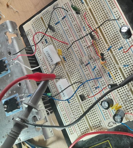
As seen above, the layout is messy, looks a bit like Frankenstein's monster but is functional. One thing to note, the VBE multiplier transistor currently isn't in contact with either of the drivers (and should be). So, the little heatsink with the output transistors on will get quite hot even if only producing 5W, or so. However, touching the VBE with my fingers I can confirm that the current starts coming down - indicating it is functioning correctly.
Below are some screen-captures of my oscilloscope showing the output signal before and after clipping.
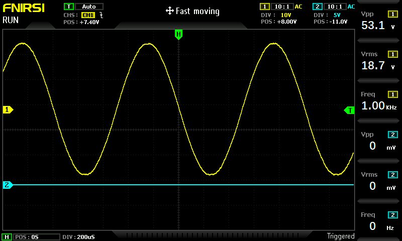
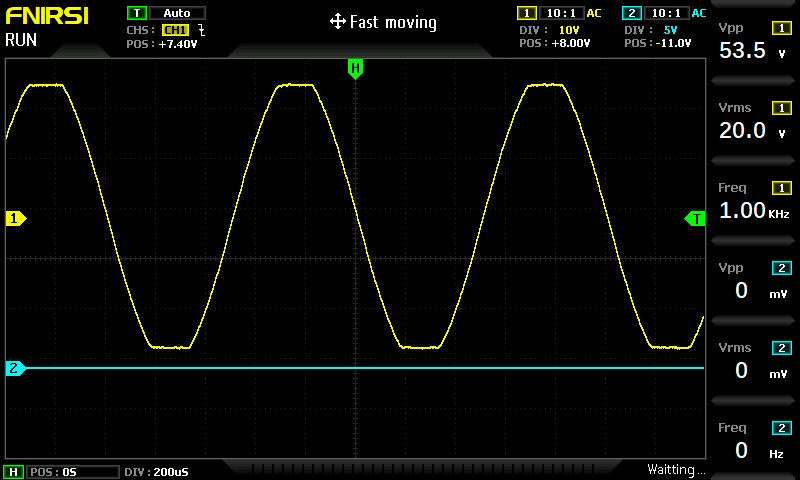
As can be seen, the output signal is nice and clean up to the 40W output power into 8 ohms. Fig. 5 shows the amplifier symmetrically clips into an 8 ohm load.
Next, I decided to deliberately capacitively-load the output of the amplifier with 20kHz square wave; first with 150n (fig. 6) and secondly 300n (fig. 7).
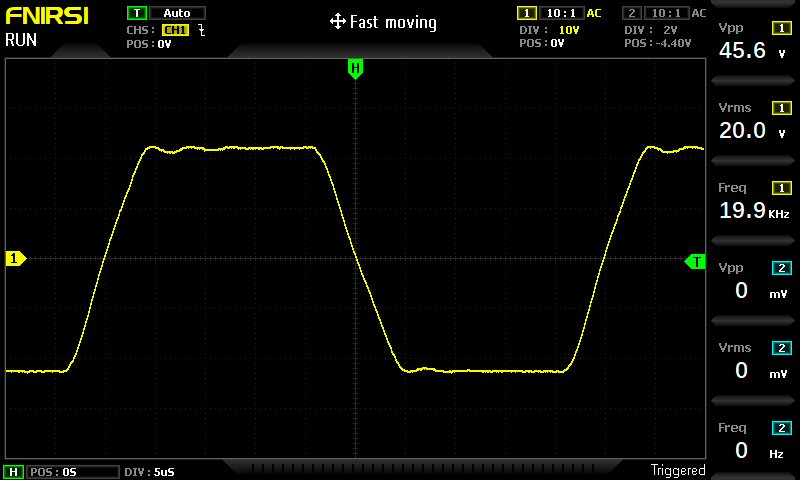
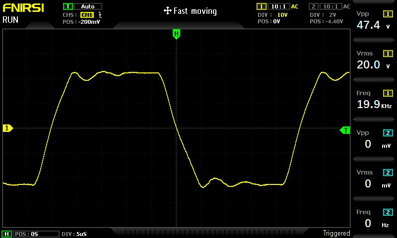
As can be seen there is an initial "hump" then dampens out almost immediately, with no visible "ringing" on the peaks. This indicates that the amplifier is stable driving difficult/capacitive loads. I decided to stop at 300n, as I only saw a slight voltage difference in the initial "hump", and pretty much the same amount of dampening as with 150n. It certainly overall wasn't worse at 300n.
Conclusion
Overall, this amplifier is an elegant example of the classic quasi-complementary topology. The long-tail pair provides accurate differential amplification, the VAS develops the majority of the voltage gain, the emitter-follower driver stage supplies the required current gain, and the quasi-complementary output stage delivers high power using two identical NPN output transistors. The inclusion of the Baxandall diode is the key feature that allows the lower half of the output stage to closely emulate the behaviour of a true complementary design, substantially reducing crossover distortion while retaining the simplicity and robustness that made quasi-complementary amplifiers popular for many years.