
This circuit is a manual DC motor speed controller that uses an NE555 timer configured to produce a Pulse Width Modulation signal. By adjusting a potentiometer, you can smoothly vary the duty cycle of the power delivered to a 12V DC motor, altering its speed from a crawl to full power.
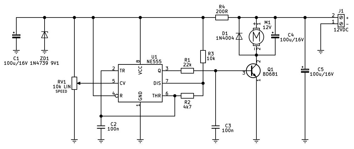
Circuit Description
The operation begins at the power supply and input regulation stage. The circuit connects to a 12V DC power source via terminal J1. A 9.1V Zener diode, designated as ZD1 (1N4739), works alongside decoupling capacitor C1 to stabilize and clamp the operating voltage supplied to the NE555 chip (U1), protecting it from voltage spikes and ensuring a clean timing reference.
Speed adjustment is handled by a 10k linear potentiometer, RV1. Unlike standard 555 astable circuits that rely on fixed internal thresholds, this design connects the wiper of RV1 directly to the control voltage pin (CV, pin 5). The internal reference thresholds of the 555 timer are normally fixed at two-thirds and one-third of the supply voltage. By turning RV1 to vary the voltage at pin 5, you actively shift these internal thresholds up or down. As the control voltage is pushed closer to the positive rail, the charging and discharging timing behavior changes, altering the duty-cycle of the square wave generated at output pin 3. Lowering the control voltage decreases the duty-cycle, slowing the motor down until it stops.
The oscillator and timing stage utilizes resistor R2 and capacitor C2 to set the baseline oscillation frequency of the timer, which is around 740Hz. Resistors R1 and R3 route the output and discharge signals from pins 3 and 7 to maintain continuous oscillation, cooperating with the modulated control voltage to produce a stable PWM pulse train.
The motor driver stage features Q1, a BD681 Darlington NPN transistor acting as a robust electronic switch capable of handling the current demands of the motor, M1. The square-wave PWM signal from pin 3 drives the base of Q1. Rather than reducing the DC voltage linearly, which would strip motors of their torque and cause stalling, the transistor rapidly switches the motor fully on and off. The percentage of time the motor is switched on during each cycle, known as the duty-cycle, dictates its effective average speed. This method is sending bursts of current to the motor controlling the speed but without reducing the torque.
Finally, protection and filtering components ensure reliable operation. A flyback diode, D1 (1N4004), is placed across the motor terminals to safely absorb and dissipate the high-voltage inductive kickbacks generated when transistor Q1 rapidly turns off, preventing damage to the semiconductor switch. Additional filtering capacitors C4, C5, and C3 smooth out voltage drops and suppress electrical noise on the power rails caused by the rapid switching of the inductive motor load, while resistor R4 provides extra decoupling between the power rail to U1 and the motor circuit.