
Note 1: article is currently under construction as of 24 July, 2026 and is subject to change once prototype has been fully tested.
Note 2: Downloadable gerber files for the PCB will be available once the design has been fully tested
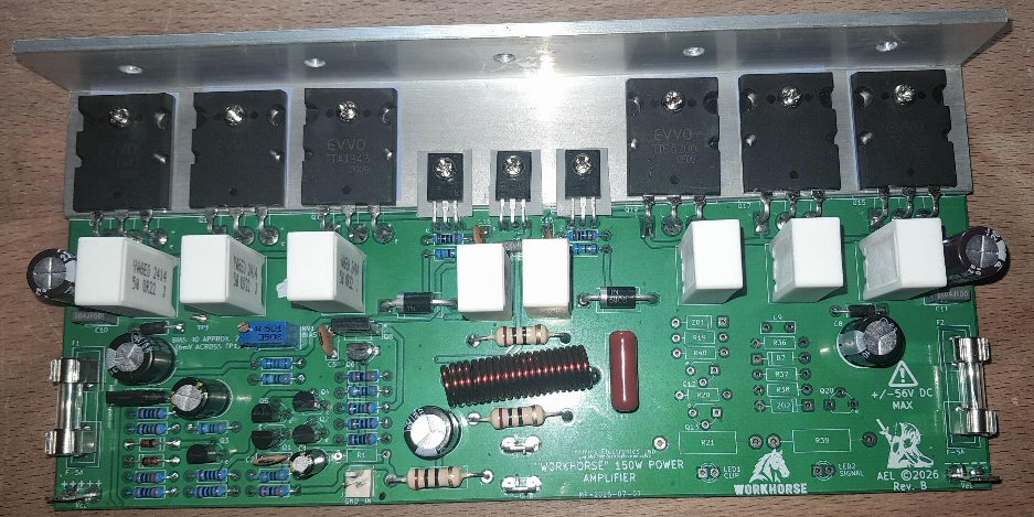
The Workhorse 150W (into 4 ohms at +/-50V DC) power amplifier is a fully complementary Class-AB audio power amplifier designed around a modern low-distortion architecture. Although the circuit is relatively straightforward, each stage has been carefully optimised so that it performs only one task before handing the signal to the next stage.
It's actually based on, and an extension of the AEL-2026 amplifier with some improvements.
The amplifier begins with a precision differential input stage, followed by a beta-enhanced voltage amplification stage, then a complementary driver stage and finally a high-current complementary feedback pair (CFP), also known as a Sziklai output stage. This arrangement provides excellent open-loop linearity, low distortion, high current capability and very good thermal stability while maintaining relatively modest component count.
The amplifier operates from split supply rails of approximately +/-50V DC nominal, allowing approximately 150W into a 4 ohm load with adequate heatsinking.
Specifications (Performance of prototype at +/-48V DC):
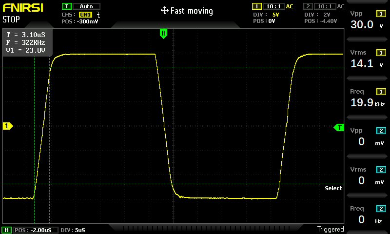
Output power: 105W into 8 ohms; 153W into 4 ohms
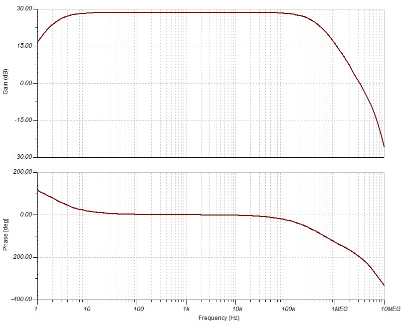
Frequency response: 15Hz - 35kHz
Total Harmonic Distortion (THD): <0.03% at full power, 8 ohms
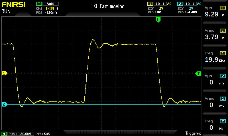
Slew rate: 7.6V/µs
Input sensitivity: 1.13V RMS
Output impedance: 0.019 ohms
Damping factor: >420
Stability: unconditional
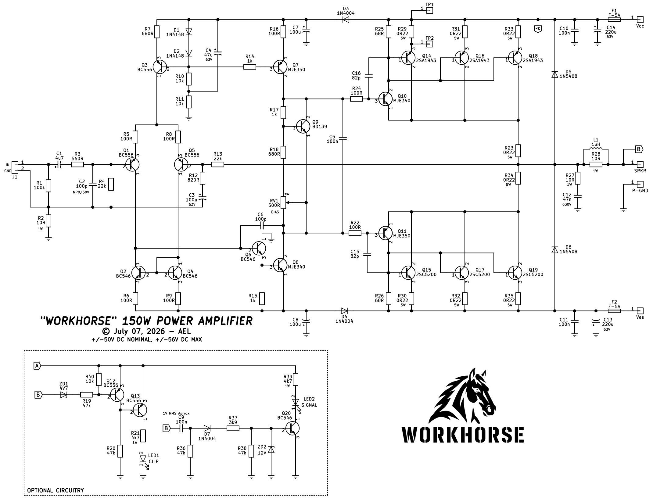
Circuit Description
The input signal enters through connector J1 and is AC coupled by capacitor C1, preventing any external DC voltage from entering the amplifier. Resistor R1 provides the input impedance, while R3 and C2 form a low-pass RF filter that prevents radio frequency interference from reaching the sensitive input stage. Resistor R4 establishes the DC operating point of the amplifier input while having minimal effect on the AC signal.
Resistor R2 is known as a "ground lift" resistor. Rather than connecting the amplifier input ground directly to the power ground, R2 inserts a small resistance between them. This helps prevent high charging currents and loudspeaker return currents from flowing through the sensitive signal ground. The result is reduced ground loop currents and lower hum, particularly when multiple amplifiers or external equipment are interconnected.
The input signal is then applied to the base of Q1, one half of the long-tail differential pair. The second transistor, Q5, receives the global negative feedback signal from the amplifier output through resistor R13. These two transistors compare the incoming audio signal against the output signal fed back from the loudspeaker terminal. Any difference between the two signals is treated as an error signal, which the amplifier attempts to reduce towards zero. This differential comparison is the foundation of the amplifier's excellent linearity.
The differential pair requires a stable tail current in order to operate correctly. This current is supplied by Q3, which functions as the constant current source for the long-tail pair. Rather than allowing the current through the differential stage to vary with supply voltage, Q3 maintains an almost constant operating current. D1, D2, R10 and R11 establish the correct reference voltage. C4 filters the reference, preventing supply ripple from modulating the input stage current.
The collector currents produced by Q1 and Q5 are processed by Q2 and Q4, which form a current mirror. Instead of using simple collector load resistors, the current mirror forces both sides of the differential pair to operate more symmetrically while converting the differential currents into a single-ended output. This significantly increases voltage gain, improves common-mode rejection and reduces even-order distortion. The current mirror also increases the effective collector load impedance, allowing the input stage to produce much higher gain than would otherwise be possible.
The single-ended output from the differential stage drives the beta-enhanced voltage amplification stage formed by Q6 and Q8. Rather than relying on a single transistor for voltage gain, these two transistors operate together to produce a much higher effective current gain. Q6 acts as the input transistor while Q8 provides the majority of the collector current. Because the current gain is effectively multiplied, the differential stage only needs to supply a relatively small base current, reducing loading and improving linearity. This arrangement allows the voltage amplification stage to swing very large voltages with excellent bandwidth while remaining highly linear.
The operating current for the voltage amplification stage is supplied by Q7, which acts as a constant current source and R16 establishes the current. Since the VAS current remains essentially constant regardless of output voltage, the voltage gain remains stable over the amplifier's operating range.
Bias for the output stage is established by Q9, which functions as the VBE multiplier or bias spreader. The adjustable resistor RV1 allows the voltage developed across Q9 to be accurately set during construction. This voltage establishes the quiescent bias current flowing through the output stage, ensuring smooth transition between positive and negative half cycles while minimising crossover distortion. Because Q9 is a transistor rather than a simple diode string, it should be mounted on the same heatsink as the output devices so that its junction temperature closely follows theirs. As the heatsink warms, Q9 automatically reduces the bias voltage, preventing thermal runaway.
The voltage amplification stage drives complementary driver transistors Q10 and Q11. These drivers provide the current gain necessary to charge and discharge the relatively large base capacitances of the output transistors without loading the voltage amplification stage. Resistors R24 and R22 act as base stopper resistors, reducing the possibility of high-frequency oscillation, while capacitors C15 and C16 provide local compensation around the driver stage to maintain stability.
The power output stage consists of transistors Q12 through Q19 connected as three complementary feedback pairs, more commonly known as Sziklai pairs. Unlike a conventional emitter follower output stage, each output transistor is driven by an opposite polarity driver transistor which forms a local feedback loop. The complementary feedback pair offers several advantages over a traditional Darlington arrangement. It provides lower saturation voltage, better thermal behaviour, reduced crossover distortion and generally superior linearity. Because each half of the output stage contains three parallel transistor pairs, the output current is shared between multiple devices, reducing stress on individual transistors while allowing the amplifier to comfortably deliver the high currents required for 150 watts of output power.
Each output transistor has its own low-value emitter resistor. Resistors R23, R25, R27, R30, R31, R32, R33, R34 and R35 ensure that current is shared evenly between the parallel output devices. Without these resistors, small differences in transistor gain or junction voltage could cause one transistor to carry a disproportionate share of the load current, potentially leading to thermal runaway.
Diodes D3 and D4 perform an important supply isolation function between the amplifier's high-current output stage and the low-current voltage gain circuitry. During large output transients, the output stage can draw several amperes from the supply rails, causing momentary voltage sag due to transformer, rectifier and reservoir capacitor impedance. Without isolation, these supply fluctuations would be coupled directly into the sensitive voltage amplification stage, reducing its available voltage swing and increasing distortion.
D3 and D4 isolate the local supply rails feeding the voltage amplification stage from these high-current disturbances, while capacitors C7 and C8 act as local energy reservoirs. During brief periods when the main supply rails dip, C7 and C8 supply the instantaneous current required by the constant current sources and voltage amplification stage, preventing the front-end from "starving" for current. Once the transient has passed and the main rails recover, the capacitors are recharged through D3 and D4.
This simple arrangement significantly improves large-signal performance, helps maintain stable operation during heavy output currents, and contributes to cleaner reproduction of fast musical transients. This is a well-established technique in higher-performance audio amplifiers because it preserves voltage gain and slew capability during demanding musical peaks. D5 and D6 protect the output stage against reverse voltage stress generated by reactive loudspeaker loads.
The amplifier output is taken directly from the junction of the complementary output stage. Before reaching the loudspeaker terminal, the signal passes through output inductor L1, with resistor R28 connected in parallel. This network isolates the amplifier from highly capacitive speaker cables and improves stability when driving difficult loads. The Zobel network consisting of R27 and C12 provides a resistive load at very high frequencies, preventing instability caused by loudspeaker inductance and cable capacitance.
Power supply decoupling is provided by capacitors C10, C11, C13 and C14, which present a low impedance to high-frequency currents and prevent supply rail modulation by large output currents. Fuses F1 and F2 protect the amplifier against catastrophic output stage failures.
The optional circuitry shown at the bottom of the schematic provides two useful status indicators. The clip detector monitors the amplifier output voltage and illuminates LED1 when clipping begins, giving a visual indication that the amplifier is being driven beyond its clean output capability. The signal detector monitors the presence of audio at the output and illuminates LED2 whenever a sufficient output signal is present, providing a simple indication that the amplifier is actively reproducing audio.
Construction details
Construction of the amplifier is relatively straight-forward, as all components mount on a single PCB (if you're using it). Start with the lower profile components first, such as the 0.5W resistors and small silicon diodes. Move on to the 1W resistors, leaving about 3mm of gap between the PCB and the body of the resistors; this assists with air-flow and prevents charring of the PCB if they ever overheat. Hardware items such as fuse clips, spade terminals and the input connector can be mounted next, followed by the MKT and ceramic capacitors. Make sure to install two 1mm PCB pins/wire stakes in TP1 and TP2. This will be used later to set the bias.
All electrolytics can be mounted next, observing correct polarity. RV1 and the small signal transistors (TO-92) can be mounted now observing the correct transistor is put in the correct place. The two larger 1N5408's can be installed (observing correct polarity) as well as the two TO-126 transistors that mount vertically. L1 can now be wound and installed which will be discussed next.
Winding L1
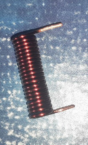
L1 consists of 20 turns of 1.25mm diameter enamel copper wire wound around the shank of a 6.5mm drill bit. Start by having 15mm of wire hanging of the end of the drill bit. Then start to wind the 20 turns around the drill bit trying to keep them as neat and as close to each other as possible. Finish off by having a 15mm length of wire hanging off the other end of the drill bit and cut off any excess. The enamel coating will need to be removed prior to installation and soldering, or the solder will not "take" (stick). See below photo for example coil.
Next, you can move on to the output stage transistors, but first, the heatsink bracket will need to be drilled.
Heatsink bracket
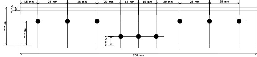
This is just a suggestion only, and I will leave how you drill the holes for the heatsink mounting face; depending on the fin spacing and type of heatsink you decide to use. Hole diameters for the transistors should be 3.5mm.
Now mount all the output, drivers and VBE multiplier transistors vertically between the bracket and the PCB using suitable hardware and insulation washers for each transistor. No collector of any transistor should be electrically connected together.
Output transistor substitutes
Even though, the original schematic denotes 2SC5200 and 2SA1943 Toshiba output transistors, a few substitutions can be used. We need to be aware that the aforementioned transistors have an ƒT (transition frequency or transit frequency) of 30MHz. So, fairly high-speed. MJL21193/MJL21194 would **work** (albeit expensive!), however they're slower in ƒT at only 4MHz, which will affect the slew rate.
TTC5200 and TTA1943 (made by EVVO Semiconductor) seem to be the genuine replacements with similar, if not better, specifications than the original in the same TO-3PL package (TO-264), which I recommend using.
Other possible substitutes (albeit package may be different) are NJW0281G for the NPN, and NJW0302G for the PNP.
Verify that each transistor is isolated from the bracket using a multimeter in continuity mode with one probe touching the bracket and touch the other probe to each transistor's collector (middle pin) down the line. There should be no continuity - if there is, find and correct the mistake.
Initial setup
It would be a good idea to use a dual channel bench supply to start off with, current limited to 200mA set to +/-30V DC. Install the fuses and rotate RV1 full counter-clockwise. This will result in minimum bias current.
If you don't have a dual channel bench supply, then you can remove both the fuses and temporarily install a 100 ohm 5W resistor across each fuse holder. This will limit the current if there's a fault condition. Connect the amplifier to a suitable +/-30V - +/-50V DC power supply.
Dual bench supply: Connect the supply leads to the amplifier and turn on the power. If it immediately goes in to current limit, then either the bias pot is installed backwards or there's another fault. Turn off the power and correct the problem.
Without a bench supply: Apply power. If the 5W resistors get very hot or even begin to smoke, there's a large current draw. Switch off **immediately** and verify the bias pot (RV1) is installed the correct way around in the circuit. Also verify everything is correctly soldered/wired (the PCB almost eliminates these problems).
The bias pot (RV1) should be wired with the counter-clockwise pin joined to the wiper and going to the emitter of Q9. The clockwise pin of the pot should go to the collector of Q9. If they're the other way around, or you've joined the wiper to the clockwise pin of the pot (if not using the PCB), the pot is backwards.
Assuming all went well, measure the DC offset between output and ground with a multimeter and verify the voltage is no higher than +/-50mV. If you see one of the supply rails, then there's an error or fault. Switch off and correct the problem.
Providing the above tests have passed, you can now remove the 5W resistors across each fuse holder (if installed) and reinstall the fuses. Connect the amplifier to a suitable +/-50V DC supply and connect a multimeter set to mV across TP1 and TP2. Switch on the power and observe the meter reading. Slowly advance the bias pot (RV1) until you see a voltage of around +/-6mV (accounting for the case the multimeter leads are backwards). This equates to a total quiescent current in the output transistors (Iq) of around 25mA.
Allow the amplifier to sit for five to ten minutes so it can thermally stabilise, and recheck the voltage reading. Re-adjust as necessary.
That's it for the initial setup. Connect up a suitable music source and speaker and give it a "listen" test.
Test results
Conclusion
Overall, the Workhorse amplifier employs a classic high-performance architecture beginning with a constant-current-fed differential input stage and current mirror, followed by a beta-enhanced voltage amplification stage, complementary driver transistors and a parallel complementary feedback pair (Sziklai) output stage. The extensive use of constant current sources, current mirrors, local feedback and global negative feedback results in an amplifier capable of delivering high output power with excellent linearity, low distortion, stable thermal behaviour and reliable operation into demanding loudspeaker loads.