
WARNING: THE FOLLOWING CIRCUIT WORKS AT AN EXTREMELY ELEVATED DC VOLTAGE OF 126V. CAUTION AND CARE SHOULD BE TAKEN AROUND SUCH VOLTAGES. IF YOU'RE UNSURE OF WHAT YOU'RE DOING OR FEEL UNCOMFORTABLE AROUND SUCH ELEVATED VOLTAGES - DO NOT ATTEMPT TO BUILD THIS.
NOTE: this has only been simulated and has not been built or tested. Stability can not be assured - treat this as a concept only. At some point I may build and test it and either update this article, or create a new one.
The idea behind this was to create a power amplifier from scratch in simulation software capable of at least 200W into 8 ohms. It was mainly born out of boredom on a Sunday afternoon. It operates from a symmetrical +/-63 V supply and is capable of delivering substantial current into a low-impedance loudspeaker load. The circuit follows the general architecture used in many high-performance discrete amplifiers, with the emphasis on keeping the individual stages simple and linear while using substantial output-device paralleling to obtain the required current capability.
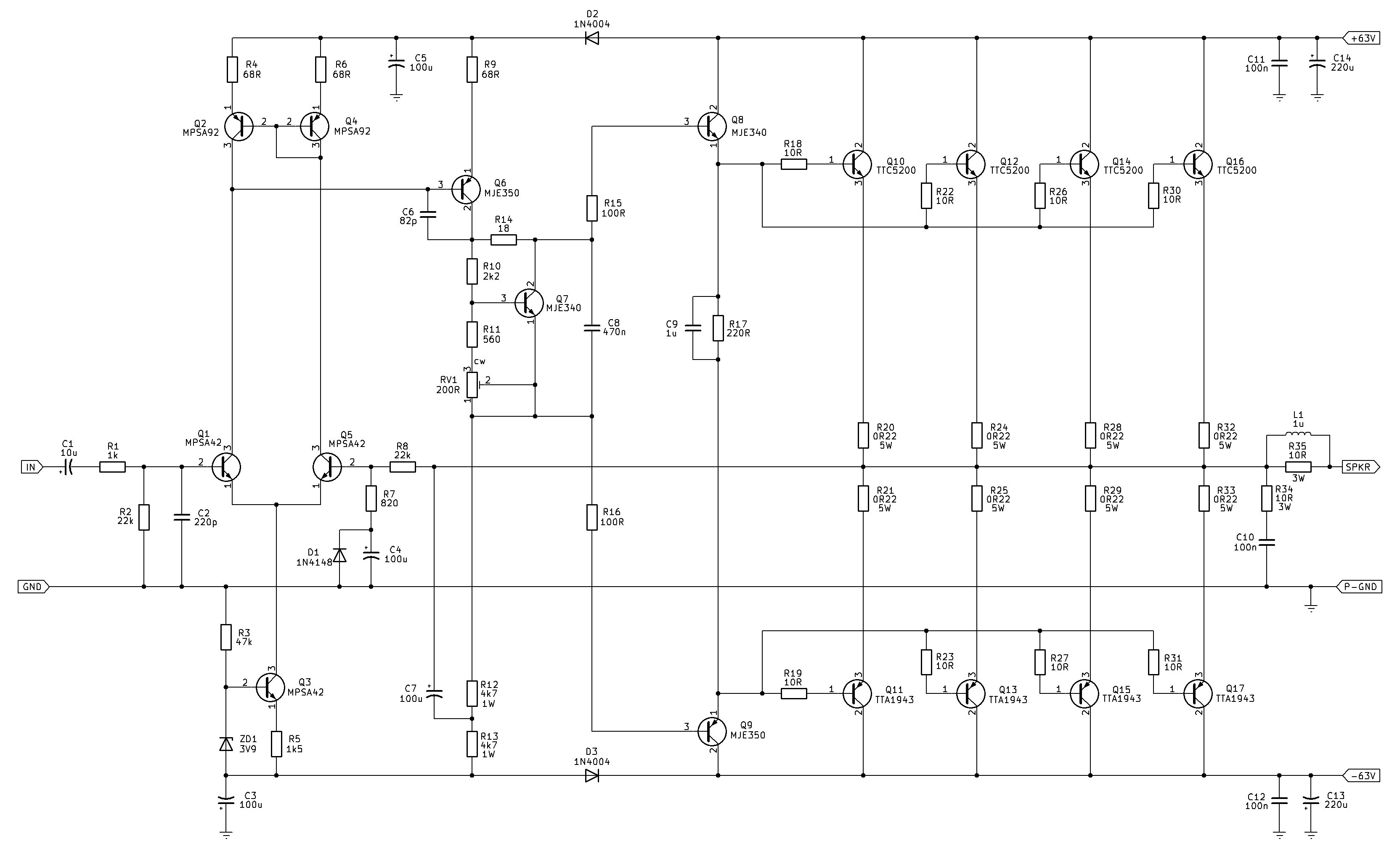
Circuit Description
The input signal is AC-coupled through C1 and applied to Q1, which together with Q5 forms the long-tailed pair (LTP). Q1 is the signal input transistor, while Q5 receives the feedback signal from the amplifier's output. The LTP effectively compares the input voltage with the feedback voltage, producing a differential current that represents the error between the two. This is the fundamental mechanism by which the amplifier maintains a very low output error and high overall linearity. R2 provides the DC return path for the input while C2 provides some high-frequency filtering at the input.
Q3 provides the approximately 1.3mA tail current for the LTP. Its base is referenced by ZD1, with R3 providing the appropriate bias current. This establishes a reasonably stable operating current for Q1 and Q5. Rather than using a resistor as the collector load of the differential pair, Q2 and Q4 form a current mirror. The current flowing in one side of the LTP is mirrored into the other side, converting the differential current into a single-ended signal for the following voltage-amplification stage. This also increases the effective gain of the input stage.
The signal from the LTP is fed to Q6, the voltage-amplification stage (VAS). Q6 provides the large voltage gain necessary to drive the output stage. Unlike many amplifier designs, the VAS here does not use a conventional constant-current source for its collector load. Instead, R12, R13 and C7 form a bootstrap arrangement. C7 follows the amplifier's output voltage and effectively causes the upper end of the VAS loading network to move with the signal. This greatly reduces the variation in voltage across the VAS load resistors and allows approximately 6.4mA to flow through Q6 with relatively little change over the output swing. One important advantage of this arrangement is that it helps reduce the asymmetry between positive and negative clipping, allowing the VAS to maintain a more similar amount of headroom in both directions.
C6 provides frequency compensation around the VAS, establishing the dominant pole necessary to make the amplifier stable when negative feedback is applied. R14 and the surrounding VAS circuitry also help control the VAS's high-frequency behaviour. The amplifier therefore has a controlled open-loop response rather than simply relying on the transistor capacitances to determine its stability.
Q7 is the VBE multiplier. Together with R10, R11 and RV1, it establishes an adjustable voltage between the bases of the upper and lower driver transistors. This voltage is approximately the sum of the base-emitter voltage requirements of the output devices and drivers, allowing the output stage to operate in Class AB rather than Class B. RV1 provides adjustment of the quiescent bias current. In a practical amplifier, Q7 should be thermally coupled to one of the driver/output devices so that the bias voltage follows temperature changes and helps prevent thermal runaway. The total quiescent current of the entire circuit should be around 120mA, which translates to around 25mA (Iq) through each output transistor.
Q8 and Q9 are the complementary driver transistors. Q8 is the upper MJE340 device and Q9 is the lower MJE350 device. They provide the current gain required to drive the substantial base currents demanded by the output transistor banks. The drivers therefore sit between the VAS/VBE multiplier circuitry and the main output devices, forming the transition from the relatively high-voltage, low-current voltage-amplification section to the high-current output stage.
The main output stage consists of four parallel complementary emitter-follower pairs. Q10, Q12, Q14 and Q16 are the upper TTC5200 NPN transistors, while Q11, Q13, Q15 and Q17 are the corresponding lower TTA1943 PNP transistors. Each complementary pair operates as an emitter follower, giving the amplifier a voltage gain of approximately unity through this section while providing a very large increase in available output current. Paralleling four pairs distributes the output current and power dissipation between eight output transistors rather than asking a single pair to handle the entire load.
The 0.22 ohm emitter-degeneration resistors, R20 through R33, are particularly important with the parallel output devices. They provide local negative feedback and encourage the output current to be shared more evenly between the parallel transistors. They also provide a small amount of ballast against differences in transistor VBE and gain. Without these resistors, one output transistor could take substantially more current than its neighbours, particularly as temperature changes, potentially resulting in thermal runaway or device failure.
The output is consequently capable of sourcing current through the upper bank and sinking current through the lower bank as the waveform alternates between its positive and negative excursions. During a positive-going signal, Q8 drives the upper TTC5200 devices harder while the lower devices turn off progressively. During a negative-going signal, Q9 drives the lower TTA1943 devices harder while the upper devices turn off. The VBE multiplier maintains a small standing voltage between the two halves so that neither side has to abruptly switch on at the zero crossing, substantially reducing crossover distortion.
D1 and D2 perform an important protective/isolation function between the input/voltage-amplification circuitry and the large output stage. During large transient conditions, the output stage can demand considerable instantaneous current. These diodes prevent the heavy output-stage currents and voltage excursions from effectively starving or disturbing the relatively small currents available to the input circuitry. D2 in particular isolates the positive supply-side circuitry from the output stage, while D3 provides the corresponding isolation on the lower side. This helps the small-signal stages maintain their operating conditions during demanding transient events.
D1 provides another protective function. C4 is part of the biasing/decoupling circuitry around the input/driver section, and under certain fault or transient conditions it could otherwise become reverse charged. D1 provides a safe path for the offending current and prevents C4 from being subjected to an undesirable reverse voltage. It is therefore primarily a protection component rather than something involved in the normal signal amplification process.
At the output, the four parallel emitter-follower pairs feed the loudspeaker through L1, a small series inductor. R35 is associated with the inductor and helps control its high-frequency behaviour, while R34 and C10 form a Zobel network from the amplifier output to ground. These components help maintain a predictable load at high frequencies and improve amplifier stability when driving the reactive impedance of a real loudspeaker and its connecting cable. C11/C14 and C12/C13 provide local high-frequency and bulk supply decoupling at the amplifier's positive and negative supply rails.
All of the electrolytic (except C1) and film capacitors should be rated at 100V DC. The ceramic capacitors are fine at 50V NP0/C0G. C1 can be replaced with a bipolar 50V type if you so wish.
Testing...
As of this time, I can provide no real support for testing this amplifier, as I have previously stated I have not built nor tested it myself. If you really do decide to build this, I would suggest sticking with a single output pair (reduces the cost if something catastrophic happens) and testing it on a dual bench supply at +/-30V with a current limit of 200 - 300mA. Start by ensuring RV1 is at maximum resistance by rotating it full anti-clockwise. This translates to minimum bias current. This is assuming you've wired the pot correctly with the anti-clockwise and center pins connected together going to to the emitter of Q7.
Apply power and look for instant current limit. Assuming it settles at around 10mA, slowly rotate RV1 until you see around 45mA (this should be about 20mA in the output pair). If while increasing the pot the current suddenly shoots to current limit, the amplifier is oscillating. This can be verified by connecting a x10 oscilloscope probe to the output point and looking for HF oscillation.
A couple of bypass 100p ceramic capacitors could be applied between each base of the driver transistors and its associated supply rail to see if this alleviates the oscillating. This is known as a "band-aid" fix - and was actually quite common to do with most EF amplifiers.
That's as far as I can go with this, and I do need to probably build and test it and update this article. Watch this space!
Simulation Results
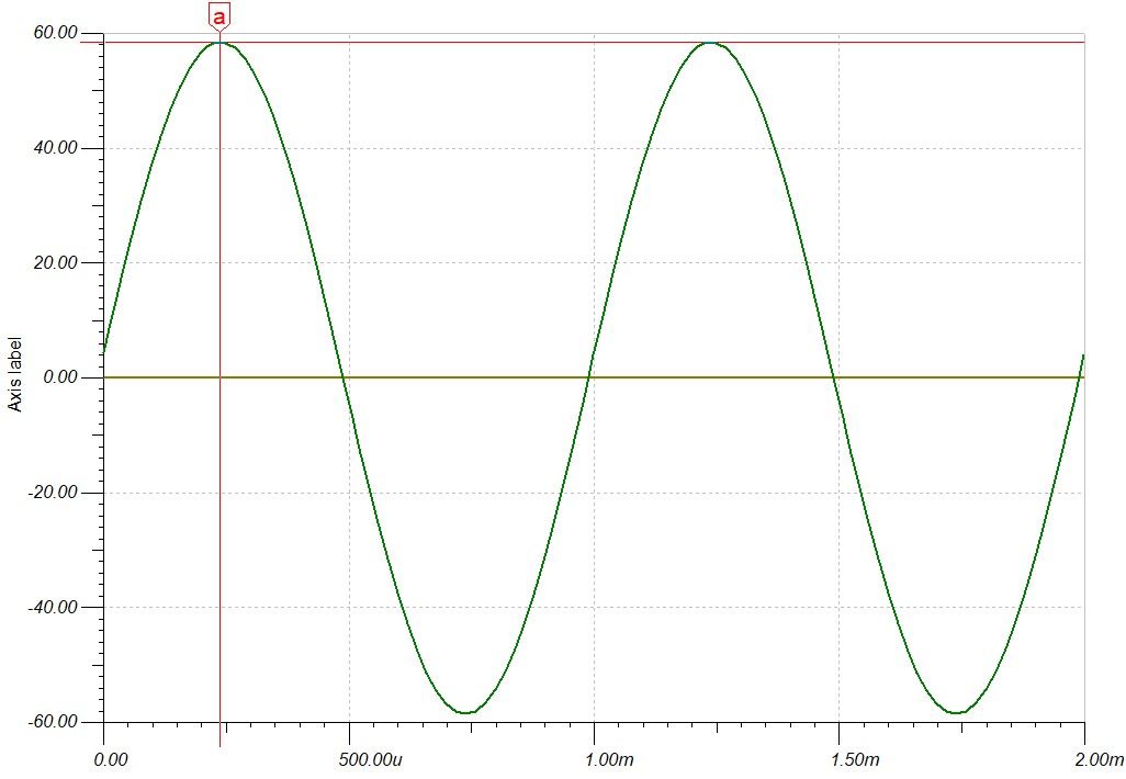
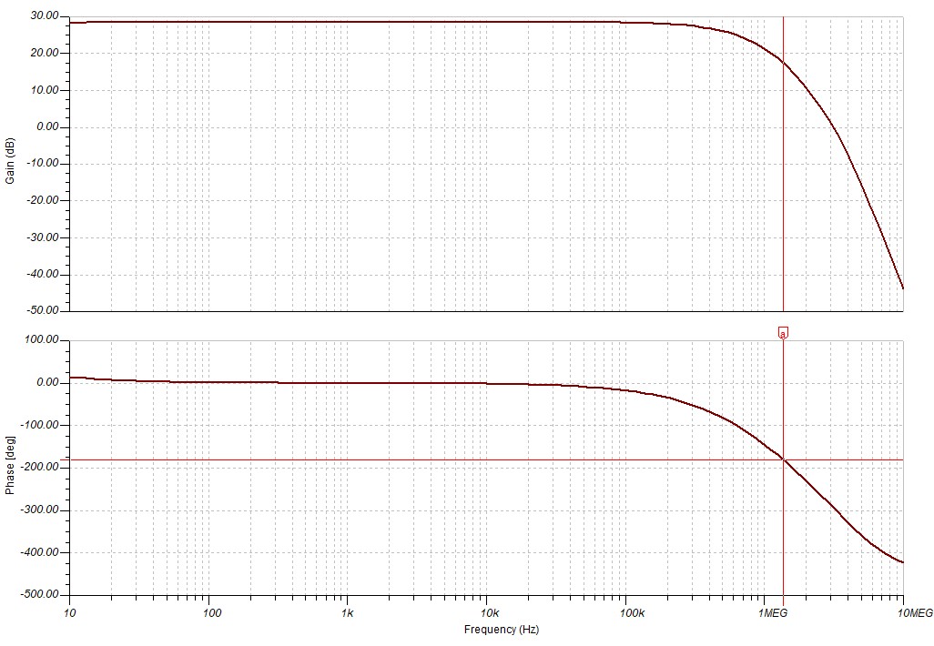
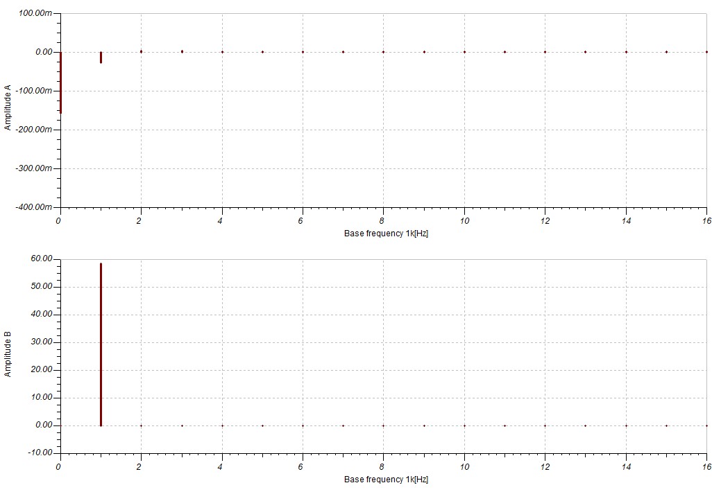
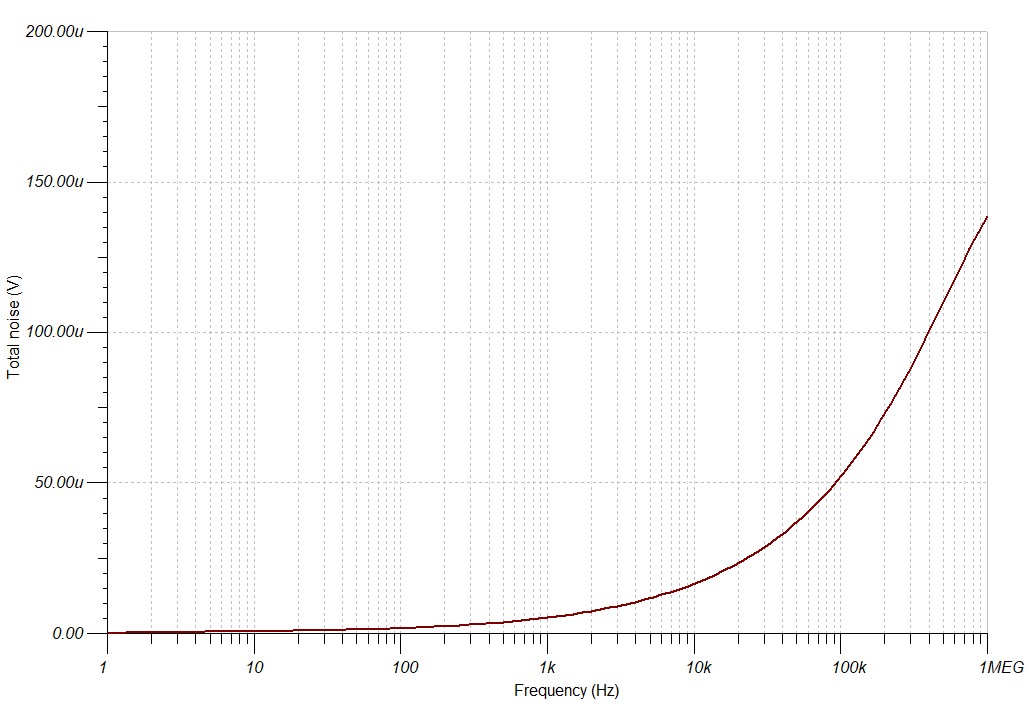
Below are some test graphs of the amplifier. Please note as this is a simulation using ideal transistors, real-world tests will differ. These should be taken as a basic representation of functionality. Also note that TINA-TI does not show oscillation - so stability of the circuit under varying load conditions cannot be confirmed.
Conclusion
I expect this amplifier will work, but again I cannot guarantee stability under varying load conditions - including unloaded. Without building and testing it to add the necessary compensation "fixes", this remains just a concept.
Overall, the circuit can be viewed as four major functional sections: Q1/Q5 form the differential error amplifier, Q2/Q4 provide its active current-mirror load and Q3 its tail current; Q6 provides the high voltage gain, with the R12/R13/C7 bootstrap arrangement supplying its approximately 6.4 mA operating current; Q7 establishes the Class-AB bias voltage; and Q8/Q9 drive the four parallel complementary output pairs. The result is a relatively conventional but very capable discrete power amplifier, with the substantial output transistor complement providing the current-handling capability while the differential input stage and global feedback provide the voltage accuracy and low distortion.