
WARNING: THE FOLLOWING CIRCUIT WORKS AT AN EXTREMELY ELEVATED DC VOLTAGE OF 126V. CAUTION AND CARE SHOULD BE TAKEN AROUND SUCH VOLTAGES. IF YOU'RE UNSURE OF WHAT YOU'RE DOING OR FEEL UNCOMFORTABLE AROUND SUCH ELEVATED VOLTAGES - DO NOT ATTEMPT TO BUILD THIS.
The following circuit is based on the concept amplifier that was tested only in simulation but never built. All the circuit operation details are in that article, so I won't repeat it here. I've nick-named this the "upside-down Blameless", as essentially it is - the input stage and VAS topology has been "mirrored".
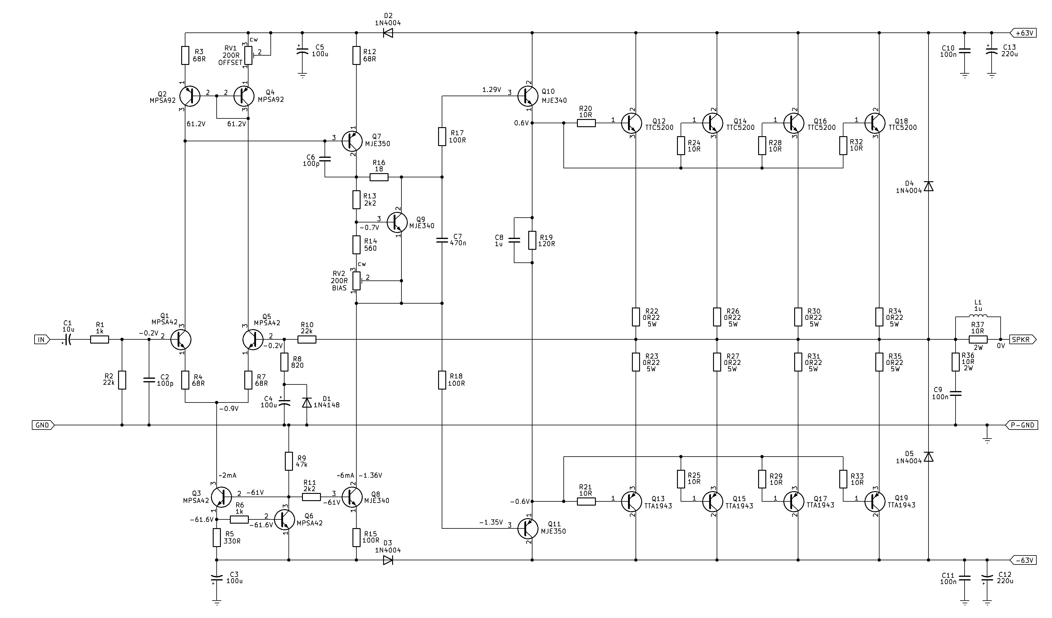
Looking at the schematic of figure 1, this is the "improved" version with only a few changes, such as the addition of a constant current source (or sink depending on how you want to look at it) for the voltage amplifier, a couple of resistor value changes and the addition of emitter degeneration resistors to the long-tail pair.
The other change was I removed the Zener diode as the voltage reference of the CCS and used a transistor instead. There are two reasons for this. Using a transistor of the same type/family as the main pass transistor for the reference network allows the VBE temperature drifts to track each other, partially canceling out temperature-induced current variations. The second reason is for lower-voltage/wider supply range. Standard Zener diodes require higher breakdown voltages (usually >2.4V or 3.3V) to operate effectively. A transistor junction or discrete active divider network can define lower reference voltages, reducing the minimum required voltage headroom (dropout).
In the terms of this amplifier, it's doubtful anyone would want to run it on a supply as low as +/-5V! The only down side to this, or any current-source for that matter, is that any fluctuation in the supply rails will cause slight variations in the output current. However, in practice, this is a moot point. So, let's get in to some real-world testing.
Front-end
To begin with real-world testing this amplifier, I'm going to start simple and test the input and voltage amplification stages separately (shown as the test circuit below) before building the output stage.
At the time of writing this part of the article, I had none of the MPSA92's. I substituted the current-mirror transistors for BC556. In this point of the circuit (and at the lower test voltage of +/-30V), the transistors aren't that critical. I will be ordering some of the MPSA92's (and some more 42's) in my next Digikey order, and before I get to the output stage. At the end of the day, I don't think it matters what transistors are used in the current-mirror - as long as the Vce of said transistors are within the SOA (safe operating area) relative to the supply rails.
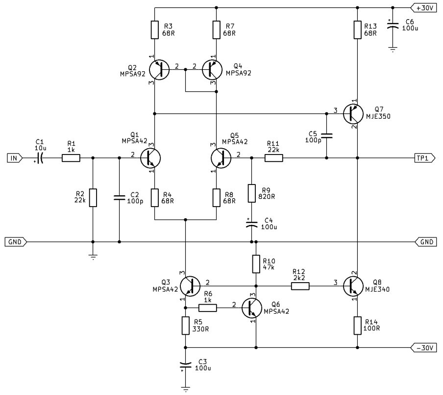
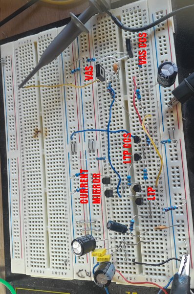
As I don't trust the accuracy of the current meters on my bench supplies, I measured the voltage drop across R5 and R14 (of figure 2) so I could calculate the currents through the LTP and the VAS. The LTP voltage drop across R5 was 592mV which calculates to V/R (0.592/330) 1.7mA, which is pretty close to the expected current of the circuit in figure 1. The VAS voltage drop across R14 measured 446mV which results in a current of 4.4mA, which is slightly under the expected current of 6mA. However, this makes sense as the voltage supply is roughly half of the voltage the final circuit will be running on. As I mentioned above, the current will vary slightly when the supply voltage varies.
Next, I measured the DC offset at TP1 and was surprised to see -12mV with un-matched transistors in the LTP. So far so good, but does it amplify? The short answer is: yes! Below are some oscilloscope captures measuring the output.
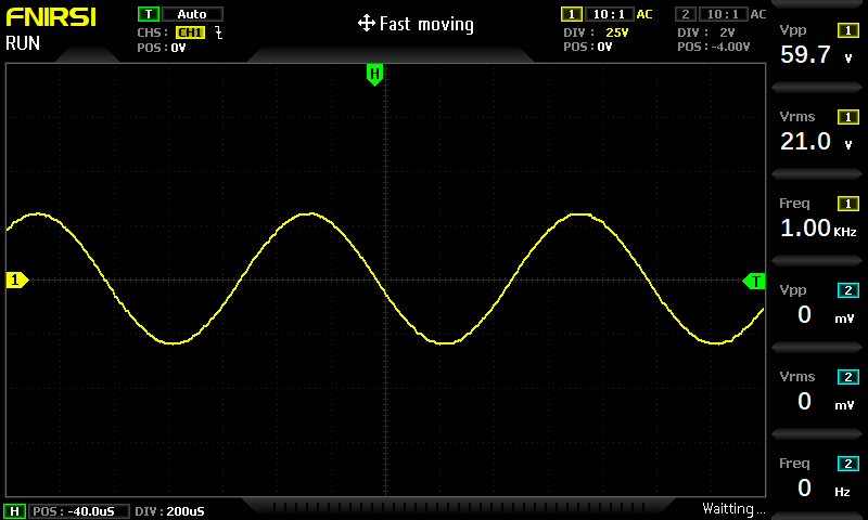
As the above shows, the output from the VAS at TP1 is clean and undistorted pushing 21V RMS; and as the peak-to-peak shows, it's very close to the supply rails.
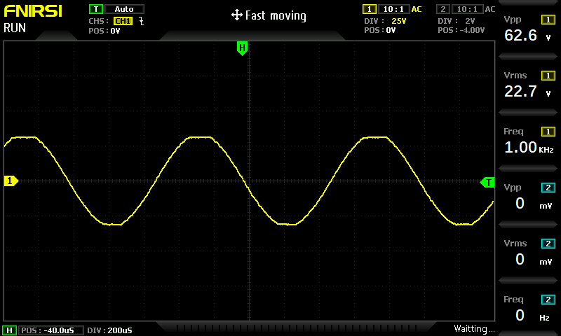
The waveform appears to clip symmetrically (or close to it) and that the voltage output is more than the supply rails. In reality this is not the case, however it does show that both the LTP and the VAS are doing their jobs nicely. More importantly, it isn't oscillating; and the Miller compensation capacitor (at this point) doesn't even need to be present - I removed it out of circuit and nothing changed. However, the collector isn't loaded; and once it is, that capacitor will become very important.
I wanted to know what the input voltage was, so I measured that next.
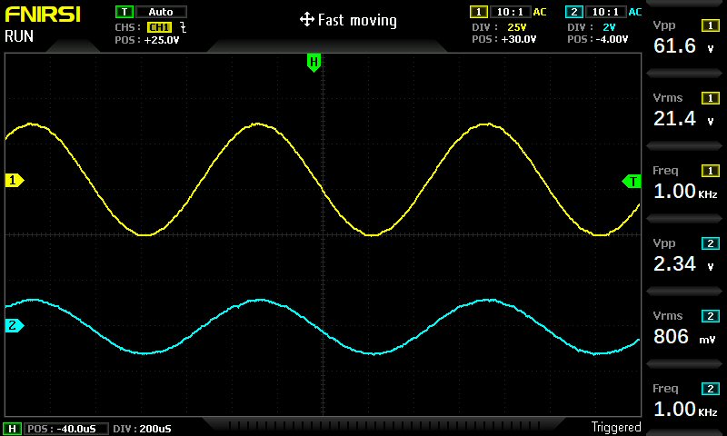
As can be seen, the upper yellow trace is our output of 21.4V RMS, and the blue lower trace is our input of 806mV RMS. This means, at the current supply voltage of +/-30V DC, the input sensitivity of the amplifier is 806mV RMS for full output undistorted.
If we divide the output RMS by the input RMS voltages (24.1/0.806) we get a gain of 26.5 (28.4dB); which is pretty close to the actual gain by dividing the resistance of R11 by R9 and adding 1 (as it's non-inverting). This equates to a gain of 27.8 (28.8dB).
I expect, however, the input sensitivity to be twice 806mV RMS (1.6V RMS, or so) at +/-60V DC.
So, the next logical step is to build the output stage, together with the VBE multiplier and verify that first, it outputs power; and second, it doesn't oscillate. If the latter is true, then I will need to investigate the issue to provide a solution. But, let's not jump the gun.
Output Stage
For the output stage, I decided to just test it with a single pair of output transistors as it will still yield useful results. After connecting it all up I was wondering why I was reaching current-limit. I'd stuck an MJE350 in place of the MJE340 driver - which is a common thing for me to do, or I end up swapping the two drivers around for whatever reason. After fixing that error, I was pleased to see with the bias pot rotated full counter-clockwise about 12mA total current draw, and the same -12mV DC offset on the output.
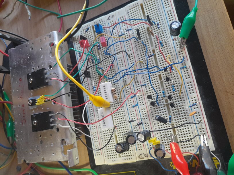
Adjusting the bias pot clockwise, I could see it was increasing evenly on the supply current meters and didn't suddenly shoot to current limit - which is usually the first sign of oscillation. Speaking of oscillation, even though my breadboard layout is absolutely terrible (see figure 5 above), with an oscilloscope connected to the unloaded output there was no signs of any on the output. Beauty! I rotated to the lowest vertical resolution and just touched the input point with my finger. I was greeted by the pleasant "blurt" on the screen.
Connecting an oscillator to the input at 1kHz (my favourite tune) with the output still unloaded, I could see a nice stable waveform on the screen with no visible signs of parasitic oscillation or distortion. Next, it was time to load it - first starting with an 8 ohm dummy load.
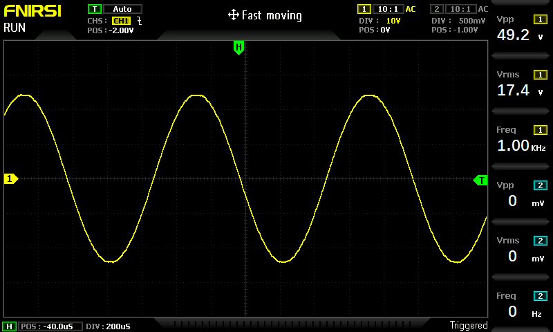
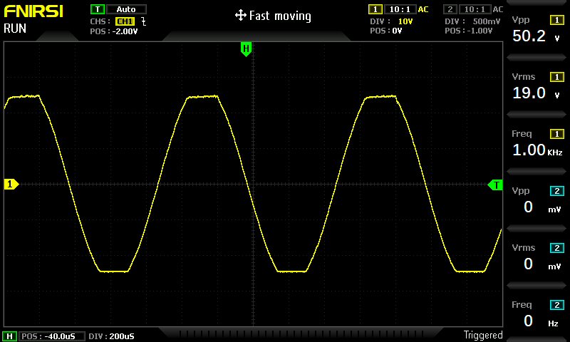
As can be seen by the two captures above, the amplifier produces a clean signal up to the onset of clipping, and (figure 7) symmetrical more or less clipping when over-driven. Next, it's the 4 ohm dummy load test.
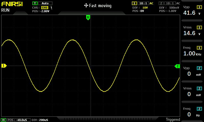
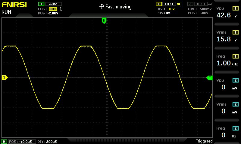
As can be seen, we get roughly the same results as we did into 8 ohm (just with less voltage RMS output). The powers at +/-30V DC are 8 ohm 37.8W and at 4 ohm 54W. Not exactly impressive, but at the supply voltage chosen for testing, it's to be expected. The next thing I wanted to test was stability. For this, I used a 20kHz square wave signal loading the amplifier into 8 ohm and deliberately placing first a 100nF capacitor across the output, then a 220nF.
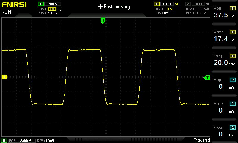
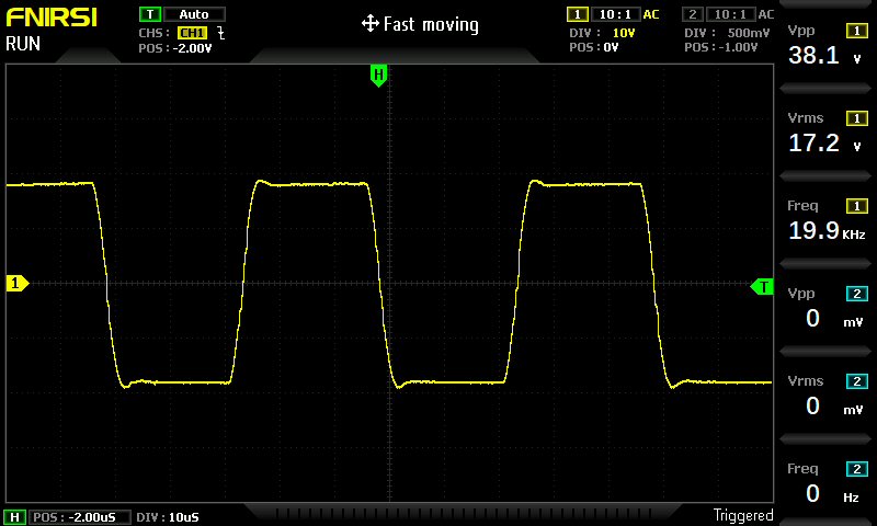
The above images show there are no visible signs of "ringing" on the output, only a small rising hump on the leading and trailing peaks. So, what does this mean now? Well, it works - straight out of the simulation without any modification (which is surprising).
The last test I wanted to do was to see how low of a supply voltage the amplifier would run on. I found that +/-5V DC would be the absolute minimum - why you'd want to run it that low, no idea; but it can. Power output into 8 ohms at that voltage is useless, though, only producing 1.57V RMS before asymmetrical clipping which is 308mW. It starts to "flat-top" first (that is the positive peak flattens out while the negative continues to be rounded. This is an indication there isn't enough voltage drive in the VAS of the amplifier. There's only 3.6mA across the emitter resistor of the CCS for the VAS - a little low. Incidentally, the LTP current is 1.4mA.
Conclusion
It works, and runs on a wide range of supply voltages. The final logical step is to design a PCB for it (which will be in the late future) and possibly write a final part 3 to this series. Watch this space!